en.Wedoany.com Reported - Researchers at ETH Zurich, led by Tobias Sagesser, have developed a scanner capable of creating high-precision 3D maps of electromagnetic fields on chips. The device uses a single beryllium ion as a sensor to measure the distribution of electric and magnetic fields near the chip surface, aiming to optimize the design and material selection of precision devices such as quantum chips.
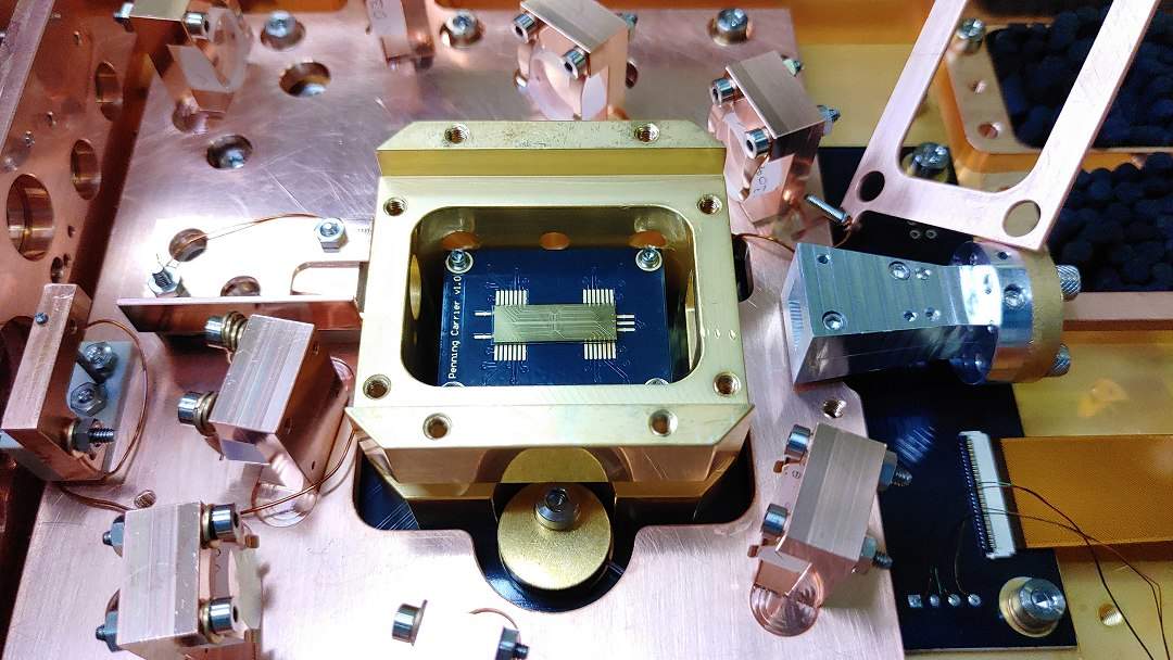
As chip miniaturization advances, particularly with the development of quantum technology, electromagnetic interference on chips has become increasingly prominent. A quantum chip may integrate up to 2 million qubits per square millimeter, and these quantum states are highly susceptible to the chip's own electromagnetic fields. The research team noted that to eliminate interference, it is first necessary to precisely measure the source and intensity of the interference.
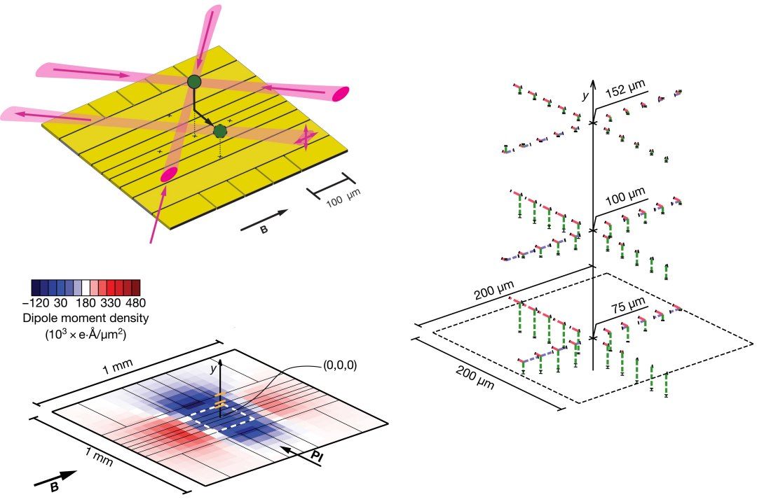
The researchers designed a sensor based on a miniaturized Penning trap. Traditional ion traps use oscillating radio-frequency electric fields, while this new trap employs a combination of static electric and magnetic fields, allowing a single ion to be moved arbitrarily in three-dimensional space. After a laser beam cools a single beryllium ion to its ground state, by adjusting the trap electrode voltages, the ion can move at heights ranging from 50 micrometers to 450 micrometers above the chip and scan an area of 200×200 micrometers. The ion jitters under the influence of the chip's oscillating electric field, and by measuring changes in its quantum mechanical oscillation state via laser pulses, the intensity of the interfering electric field can be deduced.
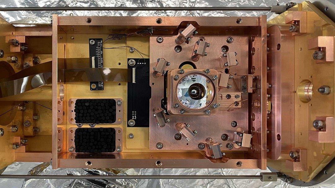
Within a one-second measurement interval, the scanner can detect electric fields with an amplitude as low as 10 nanovolts per meter. In comparison, the electromagnetic field generated by a mobile phone is ten thousand times stronger, even from several kilometers away. The researchers stated that this technology can serve as a tool for material characterization in the microelectronics industry, used to scan different areas of chips to identify low-noise materials and optimize chip manufacturing processes.