

A research team from the University of California has published findings in the Journal of Lightwave Technology, successfully achieving monolithic integration of indium arsenide (InAs) quantum-dot lasers directly onto silicon photonic chips. This advance offers a scalable solution for photonic integrated circuits (PICs) by significantly reducing optical power loss between the laser and silicon waveguides through optimized material growth and optical coupling design, thereby improving overall integration efficiency.
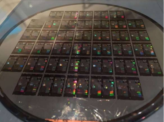
Lead researcher Dr. Rosalyn Koscica stated: "Photonic integrated circuits require more compact on-chip light sources to enable high-density integration." The team employed a two-step epitaxial growth process combined with polymer gap-filling technology to fabricate quantum-dot lasers directly on silicon substrates. Testing demonstrated stable operation in the O-band, low coupling loss, and a projected lifetime of 6.2 years at 35°C. This progress establishes a viable path toward large-scale manufacturing of silicon photonic chips.
The key advantage of this laser integration technology lies in its compatibility with existing semiconductor foundry processes and its adaptability to diverse photonic device designs. Dr. Koscica noted: "This approach can be applied to different photonic integrated circuits without complex modifications." With further optimization of silicon photonic component structures, this solution is expected to drive the widespread adoption of high-performance, low-cost on-chip light sources in the future.