

According to a study published in Nature Electronics, scientists from Boston University, University of California Berkeley, and Northwestern University have reported the world's first on-chip electronic-photonic-quantum system—a milestone for scalable quantum technology.
The system uses standard 45-nanometer semiconductor manufacturing processes to integrate quantum light sources with stable electronic devices, producing reliable streams of correlated photon pairs (light particles)—a key resource for emerging quantum technologies. This breakthrough paves the way for mass-producible “quantum light factories” on chips and large-scale quantum systems where multiple such chips work together.
“Quantum computing, communication, and sensing are still decades away from concept to reality,” said Miloš Popović, associate professor of electrical and computer engineering at Boston University and senior author of the study. “This is just a small but important step on that path, because it shows we can build repeatable, controllable quantum systems in commercial semiconductor foundries.”
“The interdisciplinary collaboration required for this work is exactly what is needed to move quantum systems from the lab to a scalable platform,” said Prem Kumar, professor of electrical and computer engineering at Northwestern University and a pioneer in quantum optics. “Without the combined efforts from electronics, photonics, and quantum measurement fields, this would not have been possible.”
Just as electronic chips are driven by electric current and optical communication links by lasers, future quantum technologies need a continuous supply of quantum light resource units to function. To achieve this, the researchers created an array of “quantum light factories” on a silicon chip, each factory smaller than 1mm × 1mm.
Generating quantum states of light on a chip requires precisely designed photonic devices—specifically, microring resonators (recently highlighted by Nvidia CEO Jensen Huang as an indispensable part of Nvidia's future expansion of AI computing hardware through optical interconnects).
To produce quantum light streams in the form of correlated photon pairs, the resonators must be synchronously tuned to the incident laser that powers each quantum light factory on the chip (and serves as fuel for the generation process). But these devices are extremely sensitive to temperature and fabrication variations, which can cause them to lose synchronization and disrupt stable quantum light generation.
To address this challenge, the team built an integrated system that actively stabilizes quantum light sources on the chip—specifically, the silicon microring resonators that generate correlated photon streams. Each chip contains 12 quantum light sources that can operate in parallel, and each resonator must remain synchronized with its incident laser even in the presence of temperature drift and interference from nearby devices (including the other 11 photon-pair sources on the chip).
“What excites me most is that we embedded control directly on the chip to stabilize quantum processes in real time,” said Anirudh Ramesh, Northwestern University PhD student who led the quantum measurements. “This is a key step toward scalable quantum systems.”
The extreme sensitivity of microring resonators—the cornerstone of quantum light sources—is well known, and it is both an advantage and a disadvantage. This sensitivity allows them to efficiently generate quantum light streams in the smallest chip area. However, even tiny temperature changes can derail the photon-pair generation process.
The Boston University-led team solved this by integrating photodiodes inside the resonators, enabling monitoring of the incident laser alignment while maintaining quantum light generation. On-chip heaters and control logic continuously adjust the resonance frequency based on drift.
“Compared to our previous work, a key challenge was pushing photonic design to meet the stringent requirements of quantum optics while adhering to the strict constraints of a commercial CMOS platform,” said Imbert Wang, Boston University PhD student who led the photonic device design. “This enabled electronics and quantum optics to be co-designed as a unified system.”
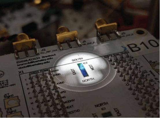
Because the chip uses built-in feedback to stabilize each source, its performance remains predictable despite temperature variations and fabrication differences—this is a fundamental requirement for scaling quantum systems. The chip was fabricated on a commercial 45-nanometer complementary metal-oxide-semiconductor (CMOS) platform, originally developed through close collaboration between Boston University, UC Berkeley, GlobalFoundries, and Silicon Valley startup Ayar Labs. Ayar Labs, born from research at the two universities, has become an industry leader in optical interconnect chips.
Through the new collaboration with Northwestern University, the same manufacturing process can now not only enable advanced optical interconnects for AI and supercomputing but—as the research demonstrates—also realize complex quantum photonic systems on a scalable silicon platform.
“Our goal was to demonstrate that complex quantum photonic systems can be fully built and stabilized within a CMOS chip,” said Daniel Kramnik, UC Berkeley PhD student responsible for chip design, packaging, and integration. “This required tight coordination across fields that typically do not communicate directly with each other.”
As quantum photonic systems continue to grow in scale and complexity, such chips could become the foundation for technologies ranging from secure communication networks to advanced sensing and ultimately quantum computing infrastructure.