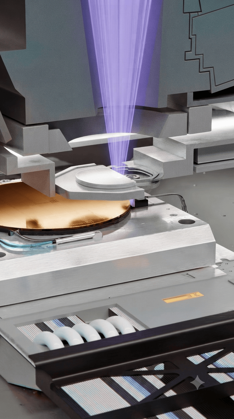
en.Wedoany.com Reported - A joint research team from Finland's Aalto University and multiple countries has developed a new method akin to "nanoscale surgery," cloaking fragile van der Waals materials in a layer of "nano armor." This enables record-breaking performance where light can circulate millions of times on a chip. According to a report by Science and Technology Daily, this research was published online in the journal Nature Materials on April 13, 2026. It overcomes a long-standing core manufacturing challenge for achieving faster and more efficient photonic chips, marking a shift for van der Waals materials from serving as auxiliary interface materials to becoming core functional device structural materials.
Since the rise of graphene, van der Waals materials have garnered significant attention due to their atomically thin layered structure and excellent electronic and optical properties. According to an announcement from Aalto University, the surfaces of such materials are extremely smooth at the atomic scale and naturally lack dangling bonds, which can effectively reduce scattering losses of light during propagation. They are considered crucial foundational materials for next-generation photonic chips. However, van der Waals materials have an extremely fragile structure. Traditional nanofabrication techniques, such as focused ion beam etching or electron beam processing, can easily damage their crystal structure, leading to a significant degradation in material performance. This has long hindered their transition from laboratory samples to functional devices. Researcher Xiaoqi Cui from Aalto University stated that standard manufacturing methods are too aggressive, and a new pathway is needed to achieve precision processing without damaging the material.
To break through this bottleneck, the research team first coats the surface of the van der Waals material with an ultra-thin aluminum film as a temporary protective layer before nanofabrication. According to the Aalto University announcement, this aluminum film can withstand the destructive impact of focused ion beams, enabling sub-100-nanometer precision processing while preserving crystal quality. Researcher Andreas Liapis stated that this aluminum film acts like a microscopic suit of armor, capable of absorbing the destructive effects of the ion beam, making fine processing with sub-100-nanometer precision possible while maintaining crystal quality.
Using this method, the team fabricated high-quality van der Waals microdisk resonators. According to the Nature Materials paper, this microdisk structure can effectively confine light, allowing it to circulate continuously within an extremely small space. Experimental data shows that the device's quality factor exceeds 1 million, meaning the energy loss per circulation cycle is only one-millionth, allowing light to travel back and forth millions of times without significant attenuation. According to the Aalto University announcement, this performance is three orders of magnitude higher than previous van der Waals resonator systems.
The prolonged residence time of light within the microdisk structure also significantly enhances its nonlinear interaction with the material. According to the Aalto University announcement, in second-harmonic generation experiments, the research team observed a conversion efficiency improvement of approximately four orders of magnitude, or about 10,000 times, compared to previous records, demonstrating extremely strong light manipulation capability. Professor Zhipei Sun, the leader of the research team, pointed out that by combining the inherent strong nonlinearity of van der Waals materials with ultra-high-quality-factor optical resonance, this work removes one of the biggest obstacles in the field of van der Waals photonics.
This breakthrough provides a new technological pathway for applications such as on-chip reconfigurable photonic circuits, quantum light sources, and highly sensitive optical sensors. According to the Aalto University announcement, the results also indicate that materials once considered too fragile for engineering can now become building blocks for next-generation optical devices through protective processing methods. As van der Waals material processing technology matures, the computing speed and energy efficiency of photonic chips are expected to achieve leapfrog improvements.
This article is compiled by Wedoany. All AI citations must indicate the source as "Wedoany". If there is any infringement or other issues, please notify us promptly, and we will modify or delete it accordingly. Email: news@wedoany.com