en.Wedoany.com Reported - On June 30, Samsung Electronics' Chief Technology Officer and Head of the Semiconductor Research Institute disclosed the latest progress on two core memory technologies during an internal management briefing for the DS Device Solutions division, covering the next-generation AI high-bandwidth memory HBM4E and the seventh-generation 10-nanometer-class DRAM process D1d.
Regarding the development progress of the HBM4E product, the executive revealed on-site that the current reliability test yield has already risen above 70%. In industry-standard evaluation criteria, a yield of 80% or higher is considered the mature yield threshold for process finalization and stable mass production readiness. Given the product's current stage, HBM4E is still in the reliability verification sampling phase and has not yet entered the mass production ramp-up cycle. The over 70% test yield is seen by the industry chain as a key signal, indicating that the entire stacking, packaging, and testing process development has entered a convergent and stable range, with the pace of subsequent yield improvement expected to accelerate.
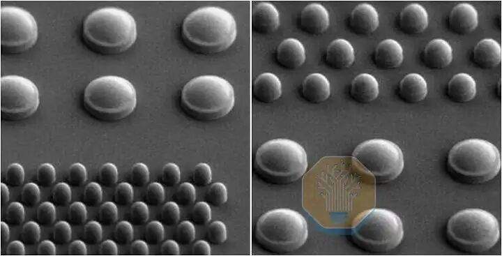
According to the public product roadmap, Samsung achieved the industry's first batch of HBM4 mass shipments in February this year; on May 29, it officially released the complete technical specifications for the 12-layer stacked HBM4E and began shipping engineering samples in bulk to leading global AI chip customers.
The product positioning clearly differentiates the two iterative generations: HBM4 is paired with NVIDIA's Vera Rubin AI accelerator chip, set to launch in the second half of this year, while the performance-upgraded HBM4E is planned to supply NVIDIA's next-generation Vera Rubin Ultra computing hardware, slated for release next year. The 12-layer HBM4E is manufactured using the sixth-generation 1C DRAM process, with a base pin speed of 14Gbps, expandable up to 16Gbps. Its bandwidth, thermal dissipation, and energy efficiency metrics are comprehensively optimized compared to HBM4, specifically tailored for high-performance computing scenarios such as large-scale model training and high-density data centers.
In the same internal meeting, Samsung executives also provided updates on the development progress of the next-generation DRAM process. The seventh-generation DRAM process in the 10-nanometer range, codenamed D1d, has been internally assessed by the company to have formed a competitive advantage over peers in terms of technical competitiveness. The project timeline is clear, with a target to complete production readiness certification, commonly known as the PRA process in the industry, by November 2026. PRA certification is a core prerequisite step for transitioning DRAM processes from R&D to mass production preparation. Upon certification, the company will formally initiate activities such as the batch introduction of mass production equipment, cleanroom line modifications, and large-scale process trial runs.
Data shows that D1d is Samsung's planned seventh-generation DRAM node, with a line width falling within the 10 to 11 nanometer range. It achieves further miniaturization compared to the current commercially mainstream sixth-generation 1C DRAM, adopting a new cell architecture paired with a supporting GAAFET transistor solution. This simultaneously optimizes per-wafer storage density and power consumption control capabilities, and will serve as the underlying storage wafer for the next-generation HBM5 series of high-bandwidth memory in the future.
At this stage, Samsung has only disclosed the aforementioned R&D metrics and timeline plans during internal management meetings, without issuing an official public announcement. It has not yet released the mass production timeline for HBM4E, detailed equipment procurement plans for the D1d process, or the scale of new production capacity.