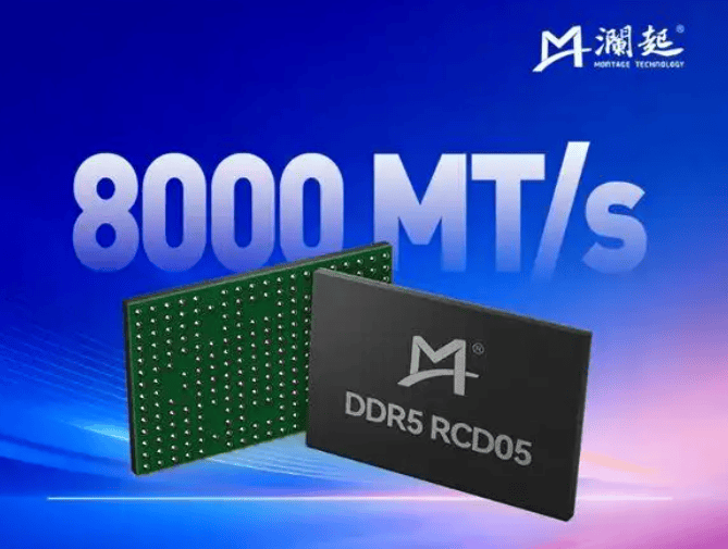
Samsung Electronics and SK Hynix Advance 16-Layer HBM4 Mass Production, Accelerating Probe Card Upgrades
en.Wedoany.com Reported - Samsung Electronics and SK Hynix announced in 2026 that 16-layer stacked HBM4 has entered the mass production ramp-up phase. As a single memory chip integrates more DRAM dies, through-silicon vias, and micro-bumps, the precision of wafer testing directly impacts final product yield. Probe cards, once considered test consumables, are becoming critical equipment for controlling scrap rates and production costs in HBM4 manufacturing lines.
Probe cards use tens of thousands of micron-scale probes to contact wafer pads, performing electrical performance testing and defect screening on chips. The 16-layer HBM4 uses vertical stacking of multiple dies, where a defect in any single layer can render the entire chip scrap. With a single-layer die yield of 97%, the cumulative yield after 16-layer stacking drops below 61%, making it essential to screen out defective dies as accurately as possible before the stacking process.
Faisal Goriawalla, Director of SLM Product Management at Synopsys, stated that data from cloud service providers has shown HBM failures are a major cause of GPU faults in data centers. HBM4 expands the memory interface to 2048 bits, further increasing the number of through-silicon vias and micro-bumps while reducing external bump pitch, imposing higher demands on probe card positioning accuracy, channel density, signal integrity, and contact stability.
Fine pitch is the most direct manufacturing challenge. HBM4 bump pitch has been compressed to below 40 micrometers, approaching 10 micrometers in some areas, requiring probe positioning accuracy within ±1 micrometer while ensuring uniform force distribution across tens of thousands of probes. Traditional cantilever probes cannot meet these requirements, making MEMS probes manufactured using photolithography and micro-electromechanical processing the primary solution for high-end HBM testing.
At the same time, HBM4 testing must handle high currents, high-speed signals, and high heat flux density. The peak power consumption of a single HBM4 stack has increased by over 50% compared to the previous generation, with a single probe card potentially carrying hundreds of amperes during testing, where localized hot spots accelerate probe wear. Data transfer rates exceeding 10 Gbps also require probe card substrates to use low-loss materials, strictly control differential line lengths and impedance continuity, and reduce signal crosstalk between adjacent channels.
The heat generated by 16-layer stacking can also cause deformation of the wafer and probe structures. A 12-inch wafer may experience warpage of approximately 200 micrometers during high-temperature testing, while HBM testing requires coverage of room temperature, high temperature, and low temperature environments. Probe materials must maintain stable contact resistance across a range from minus 40 degrees Celsius to 125 degrees Celsius. To minimize alignment deviations caused by temperature changes, high-end probe card substrates are transitioning from traditional FR-4 materials to aluminum nitride, silicon carbide, low-expansion ceramics, and glass.
Currently, high-end probe cards have evolved from simple pin boards into complex test systems incorporating space transformers, multilayer substrates, and high-density probe arrays. Aluminum nitride is primarily used for balancing heat dissipation and thermal expansion control, silicon carbide targets higher power density testing, and glass materials are suitable for high-speed signal paths. Probes manufactured using MEMS processes can control tip size, elasticity, and contact force at the micron scale, with some high-end products supporting over 500,000 contacts and certain models achieving a lifespan of one million contacts.
The global high-end memory probe card market is currently dominated by FormFactor (USA), Technoprobe (Italy), and MJC (Japan), which together control over 70% of the global market share for MEMS probe cards used in memory. Among them, FormFactor has entered the supply chains of memory companies such as Samsung Electronics and SK Hynix, with HBM4-compatible products commanding higher prices than the previous generation.
Chinese manufacturers are also advancing MEMS probe card mass production. China's QST Corporation achieved a global market share of 3.87% in 2025, ranking sixth worldwide, but its ultra-fine pitch, high-current, and high-frequency probe cards for HBM4 remain in the validation stage. As HBM production capacity expands, the competitive focus of probe cards is shifting from simply increasing probe count to a comprehensive contest in materials, thermal management, signal integrity, and micron-level manufacturing capabilities.
Related Products



Multi-function Marine Monitoring Low-altitude Detection Radar Sea-air Boundary Ocean Dynamic Environment Measurement
Chengdu Dixin Technology Co., Ltd.
GYTA Type Non-Self-Supporting Aerial/Duct Optical Cable
TONGDING INTERCONNECTION INFORMATION CO., LTD.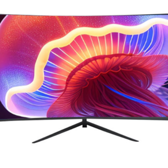
20 Inch 1600*900 Full HD 60Hz TFT LED Monitor with VGA and DP Interfaces for Desktop Computers-Business Use
Guangzhou Zanying Optoelectronics Technology Co., Ltd.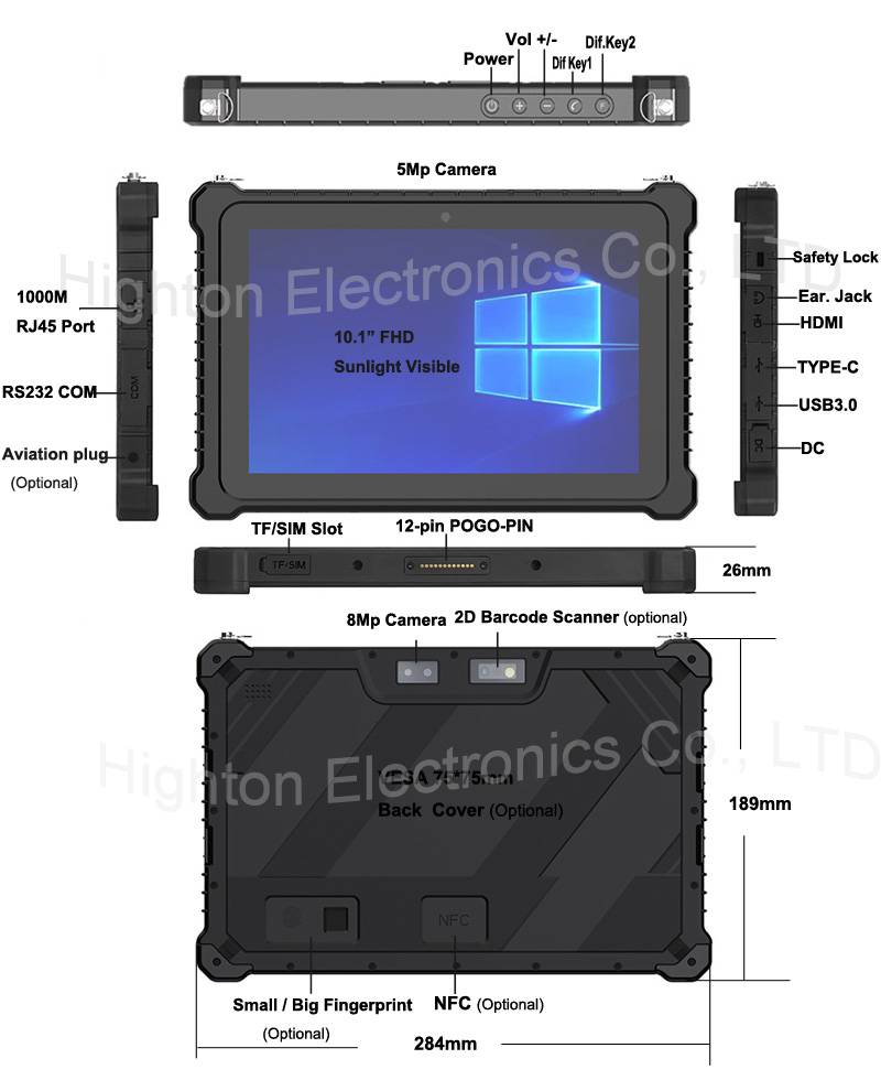
Hot Selling 10 Inch Intel N5100 I5 I7 FHD 8 +128GB 16+256GB Win10 Pro Win11 Pro 4G 5G Rugged Tablet PC Pad with NFC Barcode
Highton Electronics Co., Ltd.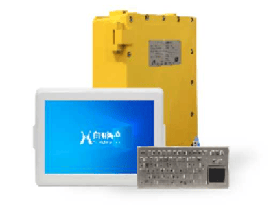
KJD127(A) Mining Explosion-Proof and Intrinsically Safe Computer
Taiyuan Xiangming Intelligent Control Technology Co., Ltd.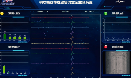
Conveyor Belt Intelligent Monitoring System
LUO YANG WIRE ROPE INSPECTION TECHNOLOGY CO., LTD.
TWP16 P-Band Tropospheric Wind Profile Radar
China Huayun Meteorological Technology Group Co., Ltd.
G.652.D Wavelength-extended Non-dispersion Shifted Single-mode Optical Fiber
HONGAN GROUP CO., LTD.