

The research team from the Irradiated Solids Laboratory published their results in Physical Review Letters, successfully developing an experimental platform that integrates nanostructure preparation with real-time characterization. This technology utilizes femtosecond laser pulses to etch nanocavities in metal thin films and synchronously employs multiple microscopy techniques for analysis, laying the foundation for developing more efficient nanoprocessing processes.
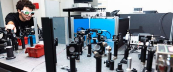
In the experiments, the researchers separated metal thin films such as nickel and iron from insulating substrates and processed them using ultrashort laser pulses with durations of about femtoseconds. Physicist Vasily Temnov from the Irradiated Solids Laboratory explained: "By changing the size and characteristics of the femtosecond laser beam, structures can be shaped, particularly the curvature of cavities." This research, through collaboration with undergraduate students from École Polytechnique, successfully combined the preparation of nanostructures with their in-situ characterization on the same platform.
This three-in-one platform synchronously adopted three characterization methods: interferometric microscopy to observe the structure formation process; photoacoustic microscopy specifically to detect cavity vibration characteristics; and magnetoplasmonic microscopy to probe the collective states of electrons. Temnov pointed out: "This is the first experiment to successfully combine all these aspects." The magnetoplasmonic technology effectively observed plasmons in nanostructures that are difficult to capture.
This breakthrough in nanoprocessing technology creates conditions for systematically studying the excitation mechanisms of various quasiparticles such as phonons, plasmons, and magnons within nanostructures. The potential demonstrated by this integrated platform provides a new technical path for future development of chip-integrated high-sensitivity pressure or magnetic field sensors.