

The advanced semiconductor material gallium nitride (GaN) is poised to become a key component for next-generation high-speed communication systems and the most advanced data centers' power electronics.
Unfortunately, the high cost of GaN and the specialized processes required to integrate this semiconductor material into traditional electronics have limited its commercial applications.
Now, researchers from MIT and elsewhere have developed a new manufacturing method to integrate high-performance GaN transistors into standard silicon CMOS chips at low cost and in a scalable way, compatible with existing semiconductor foundries.
Their approach involves building numerous micro-transistors on the surface of a GaN chip, cutting out each individual transistor, and then bonding the required number of transistors to a silicon chip using a low-temperature process to preserve the functionality of both materials.
Since only a small amount of GaN material is added to the chip, costs remain extremely low, yet the resulting device achieves significant performance improvements through compact, high-speed transistors. Additionally, by separating GaN circuits into discrete transistors that can be distributed across the silicon chip, this new technology reduces the overall system temperature.
The researchers used this process to manufacture power amplifiers, essential components in mobile phones, with signal strength and efficiency surpassing devices made with silicon transistors. In smartphones, this can improve call quality, increase wireless bandwidth, enhance connectivity, and extend battery life.
Since their method aligns with standard processes, it can enhance both existing electronics and future technologies. In the future, this new integration approach could even enable quantum applications, as GaN outperforms silicon under the low-temperature conditions required for many types of quantum computing.
"If we can reduce costs, improve scalability, and enhance the performance of electronic devices, adopting this technology is a no-brainer. We combine the best features of existing silicon materials with the finest GaN electronic components."
"These hybrid chips could revolutionize many commercial markets," said Pradyot Yadav, a graduate student at MIT and the lead author of the paper on this method. The paper was presented at the RTu2C session of the RFIC 2025 conference held in San Francisco, California, from June 15 to 17, 2025.
Swapping Transistors
Gallium nitride is the second most widely used semiconductor in the world, after silicon, and its unique properties make it ideal for applications such as lighting, radar systems, and power electronics.
This material has been around for decades, and to maximize its performance, connecting GaN chips to silicon digital chips (also known as CMOS chips) is critical. To achieve this, some integration methods bond GaN transistors to CMOS chips via soldering, but this limits the size of GaN transistors. Smaller transistors operate at higher frequencies.
Other methods integrate an entire GaN wafer onto a silicon wafer, but using so much material is extremely costly, especially since GaN is only used for a few micro-transistors. The remaining material in the GaN wafer is wasted.
"We want to combine the functionality of GaN with the powerful performance of silicon-based digital chips without sacrificing bandwidth costs. We achieve this by directly adding ultra-small discrete GaN transistors to the silicon chip," Yadav explained.
The new chip is made through a multi-step fabrication process.
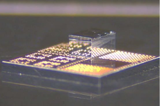
First, tightly packed micro-transistors are manufactured across the entire surface of a GaN wafer. Using highly precise laser technology, each transistor is cut to the size of a transistor, measuring 240 × 410 microns, forming so-called "dielets." (One micron is one-millionth of a meter.)
The top of each transistor is covered with tiny copper pillars, which are used to directly bond to copper pillars on the surface of a standard silicon CMOS chip. Copper-to-copper bonding can be performed at temperatures below 400 degrees Celsius, low enough to avoid damaging either material.
Current GaN integration technologies require gold for bonding, an expensive material that needs higher temperatures and greater bonding force than copper. Since gold can contaminate tools used in most semiconductor foundries, specialized equipment is typically required.
"We wanted a low-cost, low-temperature, low-stress process, and copper outperforms gold in all gold-related properties while also offering better conductivity," Yadav said.
A New Tool
To achieve this integration process, they developed a specialized new tool that carefully integrates extremely small GaN transistors with silicon chips. The tool uses vacuum suction to pick up dielets, move them over the silicon chip, and align the copper bonding interface with nanoscale precision.
They used advanced microscopes to monitor the interface, and when the dielet is in the correct position, they apply heat and pressure to bond the GaN transistor to the chip.
"In this process, I had to find new partners for each step who understood the technology I needed, learn from them, and integrate it into my platform. It took me two years of continuous learning," Yadav said.
After refining the manufacturing process, the researchers demonstrated its effectiveness by developing a power amplifier (a radio-frequency circuit that enhances wireless signals).
Compared to devices made with traditional silicon transistors, their device achieved higher bandwidth and better gain. Each compact chip has an area of less than half a square millimeter.
Furthermore, since the silicon chip used in their demonstration is based on Intel's 16 22nm FinFET advanced metallization process with passive options, they were able to integrate components commonly used in silicon circuits, such as neutralization capacitors. This significantly improved the amplifier's gain, bringing it closer to enabling next-generation wireless technologies.
"To address the slowdown of Moore's Law in transistor scaling, heterogeneous integration has become a promising solution for continuing to expand systems, reduce size, improve power efficiency, and optimize costs.
"Particularly in wireless technologies, the tight integration of compound semiconductors with silicon-based wafers is critical for achieving unified systems for next-generation antenna-to-AI platform front-end integrated circuits, baseband processors, accelerators, and memory.
IBM Research scientist Atom Watanabe (not involved in this paper) said: 'This work achieves significant progress by demonstrating the 3D integration of multiple GaN dielets with silicon CMOS, pushing the boundaries of current technological capabilities.'"