en.Wedoany.com Report on Mar 30th, ASMPT and its sub-brand O-SEMI have recently launched the new bare wafer handling system ALSI LASER1206. This fully automated laser dicing and grooving system is primarily targeted at semiconductor companies in fields such as advanced packaging, automotive power devices, and AI chip manufacturing.
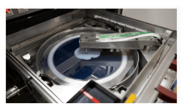
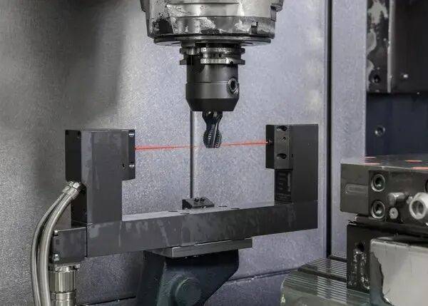
The ALSI LASER1206 utilizes patented multi-beam UV laser technology, enabling high-precision processing while minimizing thermal impact. The system supports processing various semiconductor materials including silicon, silicon carbide, and gallium nitride, and is suitable for wafer dicing and grooving processes required in advanced packaging. The equipment integrates wafer coating and cleaning stations and offers multiple automated handling options for film frames and bare wafer storage. The planar motion system features a positioning accuracy of less than 1.5 micrometers. The grooving process can handle wafers with thicknesses from 60 to 800 micrometers, while the dicing process can handle wafers from 20 to 200 micrometers thick.
In advanced packaging processes, the precision of wafer dicing and grooving directly impacts the yield and reliability of subsequent processes. The system's pre-alignment station can detect wafer notches and flat edges, achieving precise wafer alignment. The integrated coating and cleaning stations are used for protective film coating and the removal of particles and residues. ASMPT stated that this system aims to meet the increasingly complex laser processing requirements for advanced packaging processes from integrated device manufacturers (IDMs) and foundries.
Patrick Huberts, Head of ALSI Business & Marketing at ASMPT, said: "This new platform is designed to meet the hardware demands of the AI revolution. It combines high-precision laser processing with intelligent automation, supporting next-generation semiconductor manufacturing. This platform is an ideal choice for advanced packaging, AI, automotive power devices, and mobile terminal applications. It also serves as the optimal solution for pre-plasma dicing preparation to achieve high yield."
O-SEMI was established in Shanghai, China, in 2023 as a sub-brand of ASMPT, focusing on providing localized semiconductor solutions. ASMPT is headquartered in Singapore, with business covering semiconductor assembly and test, and surface mount technology. The launch of the ALSI LASER1206 system further enriches its product portfolio in the field of advanced packaging equipment.