en.Wedoany.com Reported - Samsung Electronics is refining its investment plans for a large-scale semiconductor production base in South Korea. The company plans to build four new wafer fabs by 2030, including Pyeongtaek Phase 2, Yongin Phase 1, and Gwangju Phase 1, and recently shared this plan with key partners.
According to industry sources on the 21st, Samsung Electronics recently consulted with major partners on the feasibility of its mid- to long-term wafer fab investment strategy.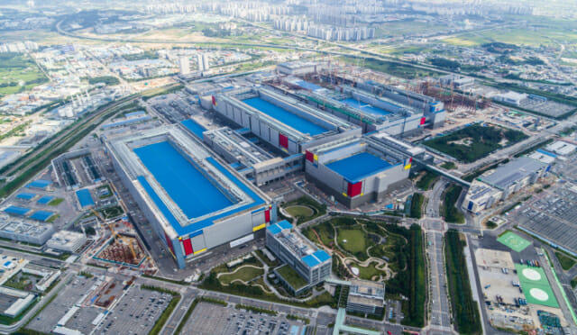
The investment plan Samsung Electronics explained to its partners includes building Pyeongtaek P5 and P6 (P5-2), the Yongin Namsa-eup semiconductor cluster Phase 1 wafer fab, and the new Gwangju Phase 1 wafer fab by 2030.
For SK Hynix, it is expected to build Y1 and Y2 wafer fabs within the Yongin Wonsam-myeon semiconductor cluster, in addition to the new Gwangju Phase 1 wafer fab. Based on this, the total number of new wafer fabs built by the two companies from this year to 2030 is expected to reach seven.
A semiconductor industry insider said that Samsung Electronics is formulating a mid- to long-term equipment investment strategy, including the southwestern region, and is conducting thorough preliminary surveys with partners, asking whether they have sufficient capacity to handle the large-scale investments of Samsung Electronics and SK Hynix.
Another source explained that Samsung Electronics is recently discussing the Gwangju investment plan with partners both online and offline. Depending on the outcome of these discussions, the pace of domestic equipment investment may accelerate faster than expected.
Previously, Samsung Electronics and SK Hynix announced a massive semiconductor equipment investment roadmap totaling 3,200 trillion won (excluding AI data center investment costs) at the "National Report on Korea's Three Major Mega Projects" held at the South Korean Presidential Office in Cheong Wa Dae.
The main content involves accelerating the equipment investment pace for existing wafer fabs under construction while significantly advancing the construction schedule for the Yongin semiconductor cluster. Samsung Electronics moved the target completion date for the Yongin wafer fab from the original 2047 to 2040, while SK Hynix moved it from 2045 to 2033. In the southwestern region, each company will invest 400 trillion won to build two memory front-end wafer fabs.
With the substantial increase in human and material resources required for large-scale equipment investment, the semiconductor industry has been concerned that the response capabilities of Samsung Electronics, SK Hynix, and related partners may face limits.
South Korean President Lee Jae-myung stated regarding the Gwangju wafer fab construction that the original plan was to proceed sequentially after completing all work in Yongin, but due to a surge in demand, he proposed advancing both simultaneously. Consequently, Samsung Electronics and SK Hynix are under pressure to push forward the Gwangju wafer fab investment as early as possible.
Analysts believe that Samsung Electronics' recent request for partners to check their investment capacity is also related to this.
A semiconductor equipment industry insider said that Samsung Electronics is recently asking partners whether they are willing to make additional local investments, based on the premise of building a wafer fab in Gwangju by 2030. However, considering current production capacity and the local infrastructure in Gwangju, it is difficult to assert feasibility.