Samsung DRAM evolves from 1α to 1β, NAND from 176 layers to 232 layers
en.Wedoany.com Reported - In the field of memory chips, DRAM and NAND Flash have adopted distinctly different technology evolution paths: DRAM continuously shrinks linewidth, while NAND keeps increasing stacking layers.
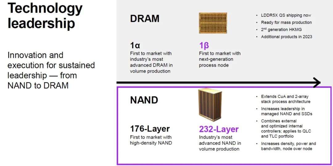
DRAM technology upgrades are primarily reflected in process nodes. Samsung's 1α and 1β are DRAM process generation codenames. 1α was the industry's most advanced mass-produced DRAM at the time and has been deployed in the market; 1β is the next-generation node, ready for mass production. Each process shrink brings higher storage density, lower power consumption, and faster speed. LPDDR5X, as a low-power DRAM standard for smartphones, is already shipping, indicating that advanced processes have been implemented in actual products.
DRAM is also introducing second-generation HKMG technology. This technology is similar to the high-k metal gate principle used in logic chips, replacing traditional silicon oxide with a high-k dielectric to reduce gate leakage and improve performance. Using HKMG in DRAM further improves refresh characteristics and power consumption, supporting higher-frequency memory interfaces.
NAND Flash technology upgrades depend on stacking layers. 176 layers and 232 layers were once industry benchmarks. 3D NAND does not rely on linewidth shrinkage but increases density by stacking memory cells layer by layer. The higher the number of layers, the more memory cells can be accommodated in the same area, reducing costs. 176 layers were first introduced to the market, while 232 layers were the advanced product mass-produced at that time.
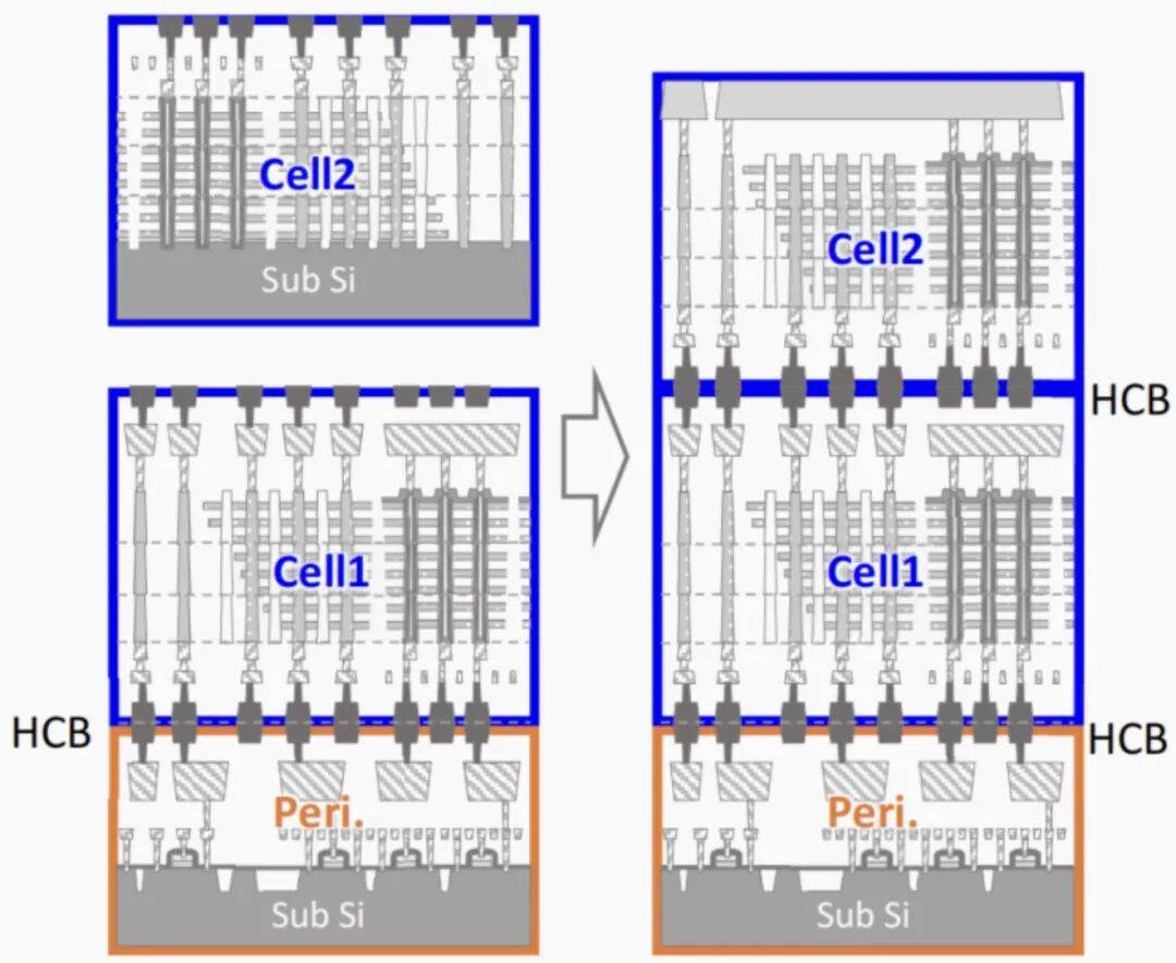
Key technologies also include CuA and dual-stack array architecture. CuA places peripheral circuits beneath the memory cells, saving chip area and improving storage density. The dual-stack array architecture interconnects two groups of memory cells stacked vertically, reducing the aspect ratio pressure of single etching and allowing further increases in layer count. The technology evolution beyond 232 layers is achieved through such architectural innovations.
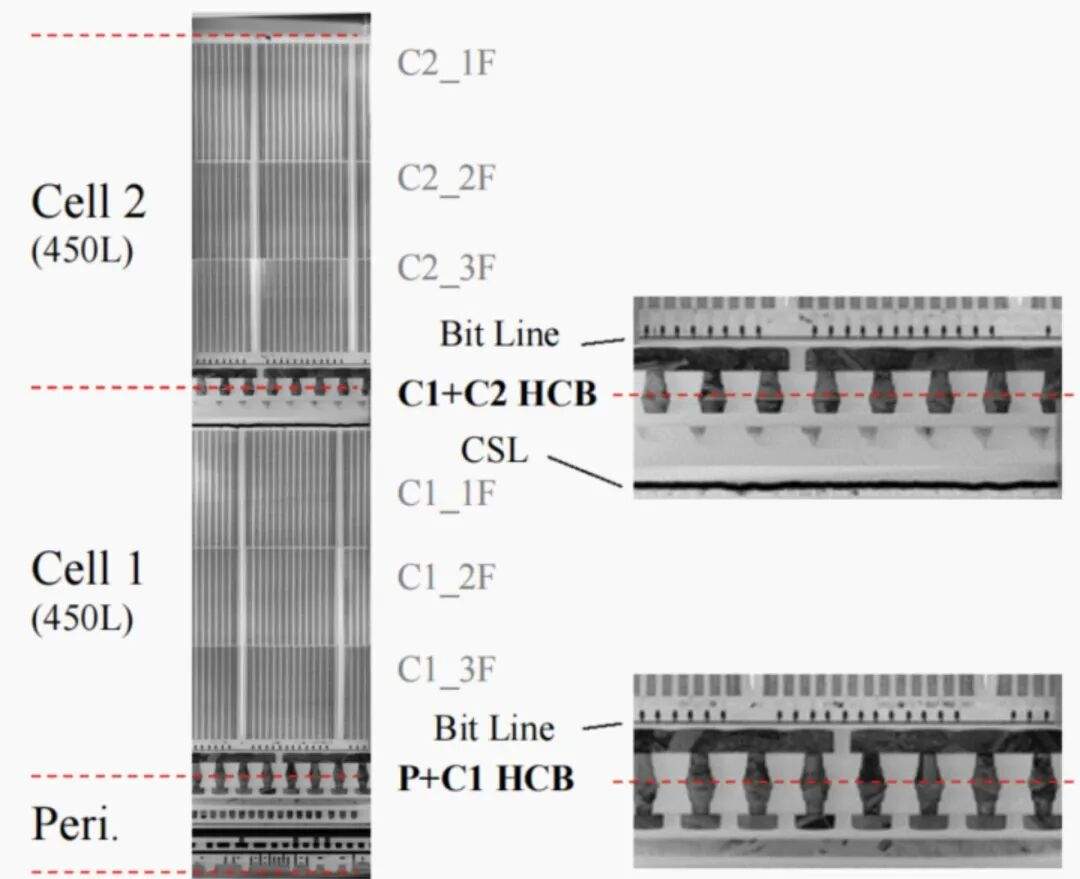
From DRAM's 1α to 1β, and from NAND's 176 layers to 232 layers, the pace of memory chip updates continues to accelerate. Each generation of process nodes and layer advancements paves the way for higher capacity, faster speed, and lower-cost data storage. Whether it is LPDDR5X in smartphones or enterprise SSDs in servers, behind them all is the result of continuous innovation by DRAM and NAND along two different paths.
Related Products


Automatic Aiming Laser Remote Obstacle Removal Robot
Pinggao Group Weihai High-Voltage Apparatus Co., Ltd.
20 Inch 1600*900 Full HD 60Hz TFT LED Monitor with VGA and DP Interfaces for Desktop Computers-Business Use
Guangzhou Zanying Optoelectronics Technology Co., Ltd.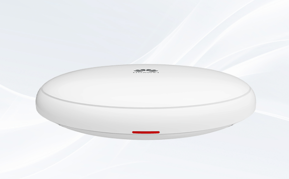
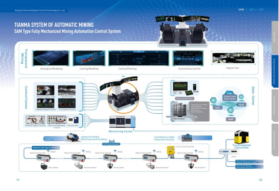
Comprehensive Mining Automation Control System
Beijing Tianma Intelligent Control Technology Co., Ltd.
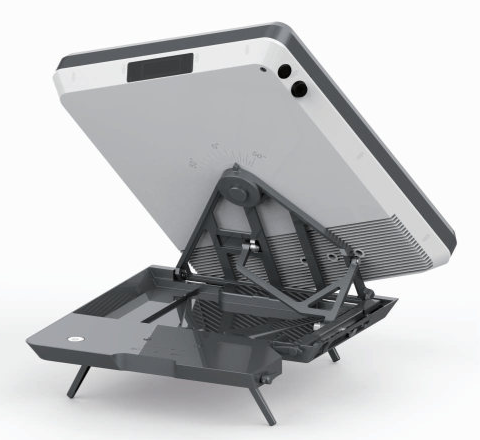
Flat Portable Satellite Terminal 0.35m Aperture Manual Portable Terminal
China Starwin Science & Technology Co., Ltd.

Multi-function Marine Monitoring Low-altitude Detection Radar Sea-air Boundary Ocean Dynamic Environment Measurement
Chengdu Dixin Technology Co., Ltd.

Industrial and Commercial Point-Type Gas Detector
Jinan Benan Technology Development Co., Ltd.