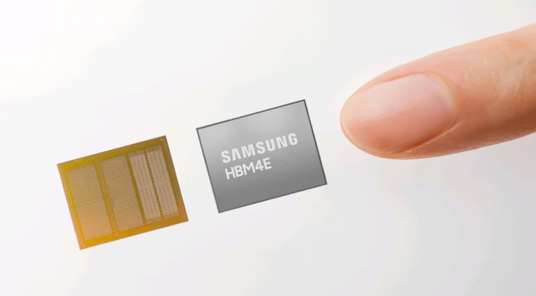
Samsung Electronics to Build DRAM Plant in Giheung with Monthly Capacity of 100,000 Wafers
en.Wedoany.com Reported - Samsung Electronics is planning to construct a new DRAM production facility at its Giheung plant in Yongin, Gyeonggi Province, converting a site originally designated for a research and development center into a memory production facility. The new plant is expected to have a monthly capacity of approximately 100,000 wafers, with an investment likely reaching tens of trillions of Korean won, and construction could begin as early as the third quarter. This adjustment in Samsung Electronics' construction plans is primarily aimed at addressing the growing demand for memory and supply shortages in the global market, driven by accelerated investment in artificial intelligence infrastructure.
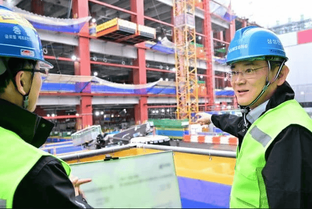
Currently, Samsung Electronics has established an internal construction organization to oversee the planning and building of the new plant. The project is comparable in scale to a single building at the nearby Hwaseong plant. To accommodate the auxiliary facilities required for the DRAM production line, the company is also considering demolishing some existing structures within the Giheung plant.
The site for the new DRAM plant was originally the location of the "SR5" building. SR5 was a landmark R&D center at Samsung's Giheung plant and the birthplace of Samsung's semiconductor business. The center was established in 1987 by Samsung Electronics founder Lee Byung-chul, who emphasized the spirit of "infinite exploration" to employees there.
As the existing facilities at SR5 could no longer meet the demands of 1-nanometer-class ultra-fine processes and cutting-edge memory R&D, Samsung Electronics management demolished the building between late last year and early this year.
According to previous plans, after the demolition of SR5, Samsung Electronics intended to build two new R&D center buildings on the site, serving as the "R&D control tower" for the Giheung plant, similar in function to the DSR Tower at the nearby Hwaseong plant. With the expansion of the Device Solutions division, which oversees Samsung Electronics' semiconductor business, and an increase in R&D personnel, the company had originally planned to further expand R&D space by constructing new R&D centers.
However, amid the rapid growth of global AI infrastructure investment and tightening supply in the memory market, Samsung Electronics ultimately adjusted its original plan, repurposing the site from an R&D center to a memory production facility.
Recently, global IT companies have accelerated the construction of large-scale AI computing data centers, driving sustained growth in memory demand. In particular, as DRAM manufacturers struggle to fully meet the demand for high-bandwidth memory, general-purpose memory used in smartphones and personal computers has also begun to experience supply constraints.
Market research firm Counterpoint Research estimates that, driven by rising product prices, global DRAM market revenue will increase from $150 billion to $210 billion this year, equivalent to approximately 312 trillion Korean won.
With expanding market demand, Samsung Electronics is accelerating efforts to boost semiconductor production capacity. An industry insider noted that Samsung Electronics' operating profit exceeded 140 trillion Korean won in the first half of this year alone, and the company is currently seeking opportunities to increase capital investment. Industry analysis suggests that, compared to continuing with R&D center construction, Samsung Electronics management is now placing greater emphasis on rapidly expanding production capacity to meet the growing demand for memory.
In addition to planning the new DRAM plant at the Giheung facility, Samsung Electronics is also expanding semiconductor production capacity centered on its Pyeongtaek plant. A new production line is being built at Pyeongtaek Plant 4, with plans to produce 100,000 DRAM wafers per month for the sixth-generation high-bandwidth memory HBM4.
Samsung Electronics also plans to build a new plant in Yongin, Gyeonggi Province, positioning it as a next-generation semiconductor cluster, with a target operational date of 2029. Furthermore, the company is constructing a second advanced semiconductor plant within the semiconductor cluster in Gwangju, South Jeolla Province, with a planned investment of 400 trillion Korean won.
Related Products

Automatic Aiming Laser Remote Obstacle Removal Robot
Pinggao Group Weihai High-Voltage Apparatus Co., Ltd.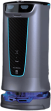
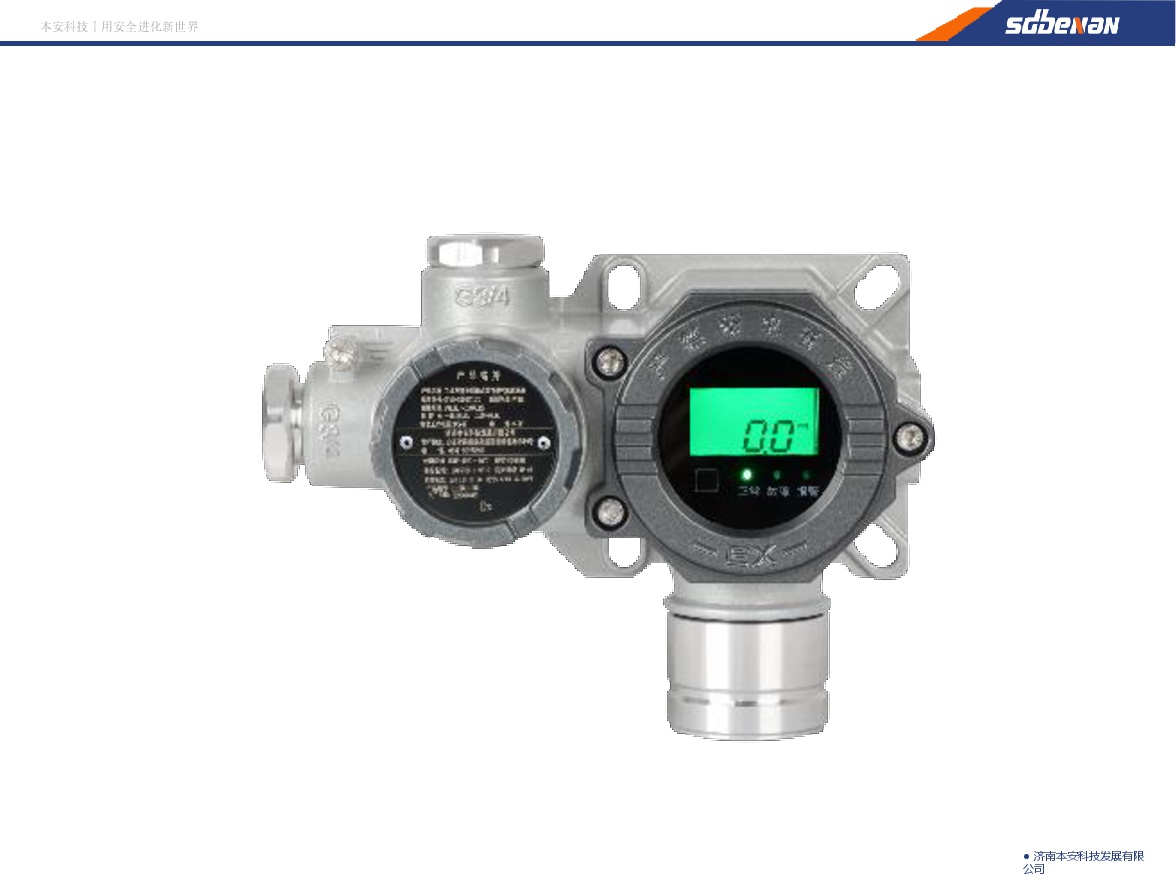
Industrial and Commercial Point-Type Gas Detector
Jinan Benan Technology Development Co., Ltd.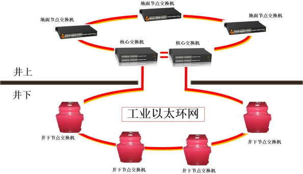
Mine Explosion-proof and Intrinsically Safe Industrial Ethernet Ring Network (10 Gigabit/Gigabit)
Chongqing Mas Sci&Tech Co., Ltd.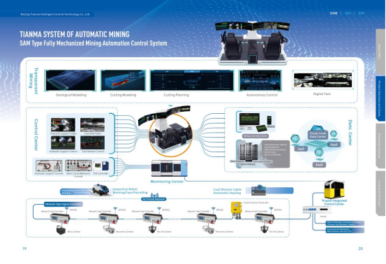
Comprehensive Mining Automation Control System
Beijing Tianma Intelligent Control Technology Co., Ltd.
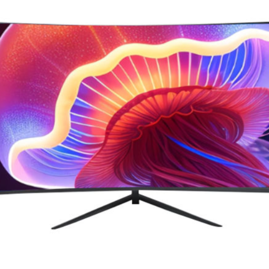
20 Inch 1600*900 Full HD 60Hz TFT LED Monitor with VGA and DP Interfaces for Desktop Computers-Business Use
Guangzhou Zanying Optoelectronics Technology Co., Ltd.
TWP16 P-Band Tropospheric Wind Profile Radar
China Huayun Meteorological Technology Group Co., Ltd.
Multi-function Marine Monitoring Low-altitude Detection Radar Sea-air Boundary Ocean Dynamic Environment Measurement
Chengdu Dixin Technology Co., Ltd.
Conveyor Belt Intelligent Monitoring System
LUO YANG WIRE ROPE INSPECTION TECHNOLOGY CO., LTD.