Samsung Electronics builds production line with 50 hybrid bonders at Pyeongtaek campus, to launch by year-end
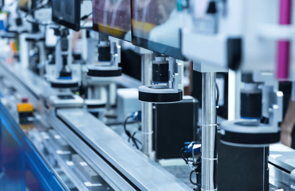
en.Wedoany.com Reported - Samsung Electronics is building a mass production line equipped with 50 sets of chip-to-wafer (D2W) hybrid bonding units at its Pyeongtaek campus for the production of next-generation high-bandwidth memory (HBM) and logic semiconductors. Equipment delivery and installation are expected to begin by the end of this year.
According to the semiconductor industry on the 21st, Samsung Electronics has selected Dutch semiconductor back-end equipment company BESI as its primary partner and has begun procuring 50 D2W hybrid bonders. These devices are planned to be installed on the mass production line at the P5 plant on the Pyeongtaek campus. Vesh CEO Richard Blickman stated during the first-quarter earnings call in April last year that more specific details about the hybrid bonder would be disclosed by mid-year. At that time, Vesh's hybrid bonder was undergoing quality verification by Samsung Electronics.
However, finalizing the order will still take more time. Due to Samsung Electronics' request for structural modifications to the equipment, a specific delivery timeline has not yet been determined. Structural modifications involve adjusting specifications such as equipment design, components, or modules to meet customer requirements. Additionally, Vesh's hybrid bonder is priced at approximately 6 billion Korean won, about twice that of competitors, a factor believed to have prolonged negotiations. An industry insider noted that Vesh supplies hybrid bonders to global semiconductor companies including TSMC and Micron, but modifying the equipment structure solely to meet Samsung Electronics' demands has put significant pressure on the company. While Samsung Electronics considers Vesh's equipment the best option, it is also exploring products from domestic equipment manufacturers with faster response times due to coordination difficulties.
Samsung Electronics' semiconductor equipment subsidiary SEMES has also secured an order to supply D2W hybrid bonders for the mass production line. The company plans to build two hybrid bonding mass production lines at the Pyeongtaek campus. Another industry insider pointed out that SEMES was initially tense when Samsung Electronics chose Vesh equipment, but the situation has recently improved. SEMES completed the development of its D2W hybrid bonder earlier this year and has delivered it to Samsung Electronics for performance verification. The equipment is understood to have passed testing.
Samsung Electronics is also considering Hanwha Semiconductor as a partner for its hybrid bonders. Hanwha Semiconductor completed the development of its second-generation D2W hybrid bonder "SHB2 Nano" in February this year and provided evaluation products to SK Hynix in April last year. This product is an integrated system (cluster) comprising a bonder, Cymex's wafer transfer module (EFEM), Hanwha Semiconductor's plasma activation module, and Zeus's cleaning module.
The D2W hybrid bonding mass production line being built by Samsung Electronics at the Pyeongtaek campus is directly related to the packaging processes for HBM and logic semiconductors. According to industry sources, in addition to the Cheonan semiconductor back-end packaging center, Samsung Electronics is also preparing a next-generation HBM hybrid bonding line at the Pyeongtaek campus. Using hybrid copper bonding (HCB) technology instead of traditional thermocompression (TC) bonding to stack HBM core chips (DRAM chips) can significantly improve performance, reduce power consumption, and lower heat generation. This is because directly bonding copper and dielectric layers eliminates the need for metal bumps (microbumps), thereby shortening the interconnection length between devices.
This technology is highly likely to be applied to customer-customized HBM (cHBM) chips. Samsung Electronics replaces the base chip of cHBM with a logic chip carrying the customer's computing circuits (IP), which assists external central processing units (CPUs) and graphics processing units (GPUs) in computation and optimizes data transmission. Samsung Electronics plans to adopt a 3D system-in-package (SiP) structure, vertically stacking HBM DRAM layers on top of the logic chip. Last month, Samsung Electronics' foundry center unveiled the next-generation 3D vertical stacking solution "3D Cube-H" based on hybrid bonding technology. This is a heterogeneous integration packaging technology designed for next-generation artificial intelligence (AI) chips and high-performance computing (HPC) systems. Compared to existing packaging technologies, it offers higher performance, energy efficiency, and bandwidth. Samsung's foundry center is actively promoting the application of this technology to customers.
Starting from the end of this year, hybrid bonders from equipment manufacturers are expected to arrive at the Pyeongtaek campus for installation. However, internal predictions at Samsung Electronics suggest that mass production of hybrid bonding technology will not be achieved until 2030, due to its higher technical difficulty compared to thermocompression bonding. Industry insider C predicted: "We expect hybrid bonding technology to be fully adopted around 2029, coinciding with the release of NVIDIA's next-generation AI accelerator, Feynman."
Related Products

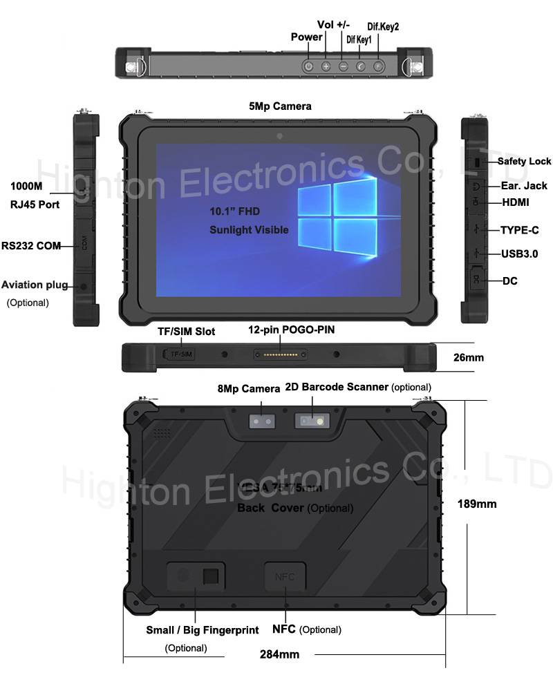
Hot Selling 10 Inch Intel N5100 I5 I7 FHD 8 +128GB 16+256GB Win10 Pro Win11 Pro 4G 5G Rugged Tablet PC Pad with NFC Barcode
Highton Electronics Co., Ltd.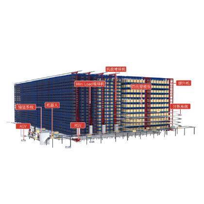
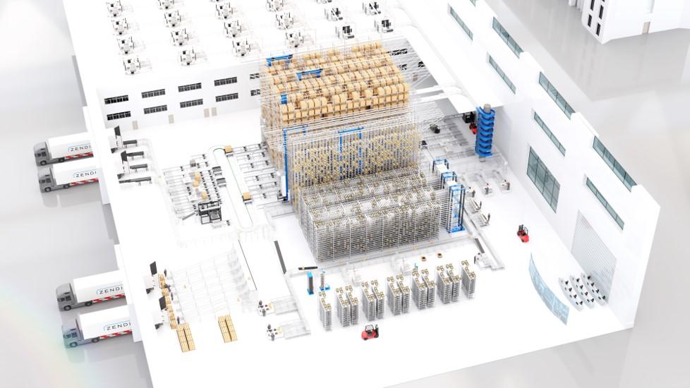
One-Stop Steward Service for the Entire Logistics System Integration Chain
Zhongding Intelligent (Wuxi) Technology Co., Ltd.
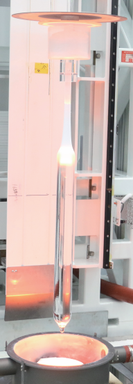
G.652.D Wavelength-extended Non-dispersion Shifted Single-mode Optical Fiber
HONGAN GROUP CO., LTD.

MUX Series Communication Interface Device for Security and Stability Control System
Nanjing NR Electric Co., Ltd.
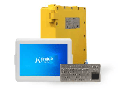
KJD127(A) Mining Explosion-Proof and Intrinsically Safe Computer
Taiyuan Xiangming Intelligent Control Technology Co., Ltd.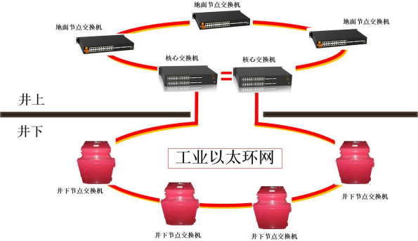
Mine Explosion-proof and Intrinsically Safe Industrial Ethernet Ring Network (10 Gigabit/Gigabit)
Chongqing Mas Sci&Tech Co., Ltd.