en.Wedoany.com Reported - On July 15, Samsung Electronics announced plans to build a new DRAM wafer fabrication plant at the Giheung Semiconductor Complex in Yongin, Gyeonggi Province, South Korea. The facility is planned to have a monthly production capacity of approximately 100,000 wafers, with an estimated investment of tens of trillions of Korean won. Construction could begin as early as the third quarter of 2026. The information disclosed so far remains at the planning stage, and specific details such as the exact investment amount, process technology, and production timeline are yet to be confirmed by Samsung Electronics.
Based on a simple calculation of a monthly capacity of 100,000 wafers, the annual wafer input capacity of this semiconductor plant at full production would be approximately 1.2 million wafers. The new capacity will enable the Giheung complex to once again undertake larger-scale DRAM production tasks and expand Samsung Electronics' supply capability of memory chips for the AI server, data center, and consumer electronics markets. However, current reports have not disclosed which generation of process technology the new plant will adopt, nor have they clarified whether all capacity will be used for high-bandwidth memory. Therefore, it cannot be directly identified as a wafer fabrication line dedicated to HBM production.
The area designated for the proposed semiconductor plant was originally planned for expanding research and development facilities. With the increase in investment in AI infrastructure and the rising demand for server DRAM and high-bandwidth memory, Samsung Electronics is reportedly deciding to repurpose part of the land, converting the original R&D facility plan into a large-scale production facility. To meet wafer manufacturing needs, the company may also demolish some existing buildings within the Giheung complex to free up space for auxiliary facilities, power systems, and production support engineering.
The proposed DRAM plant is not the same project as the existing NRD-K semiconductor R&D center in the Giheung complex. NRD-K covers approximately 109,000 square meters, and Samsung Electronics plans to invest about 20 trillion Korean won by 2030. The dedicated R&D production line was originally scheduled to begin operations in mid-2025, primarily focusing on the development of next-generation memory chips, system semiconductors, and wafer manufacturing processes. The new plant, on the other hand, is positioned to expand commercial production capacity, with a focus on achieving a large-scale supply of approximately 100,000 wafers per month.
Samsung Electronics has also been advancing other memory chip capacity projects recently. The company is expanding advanced DRAM production lines at the Pyeongtaek complex and plans to advance the operation timeline of the first wafer fab in the Yongin semiconductor cluster to 2029. If the Giheung new plant proceeds as planned, it will join the Pyeongtaek and Yongin production bases to form Samsung Electronics' latest round of wafer manufacturing expansion layout.
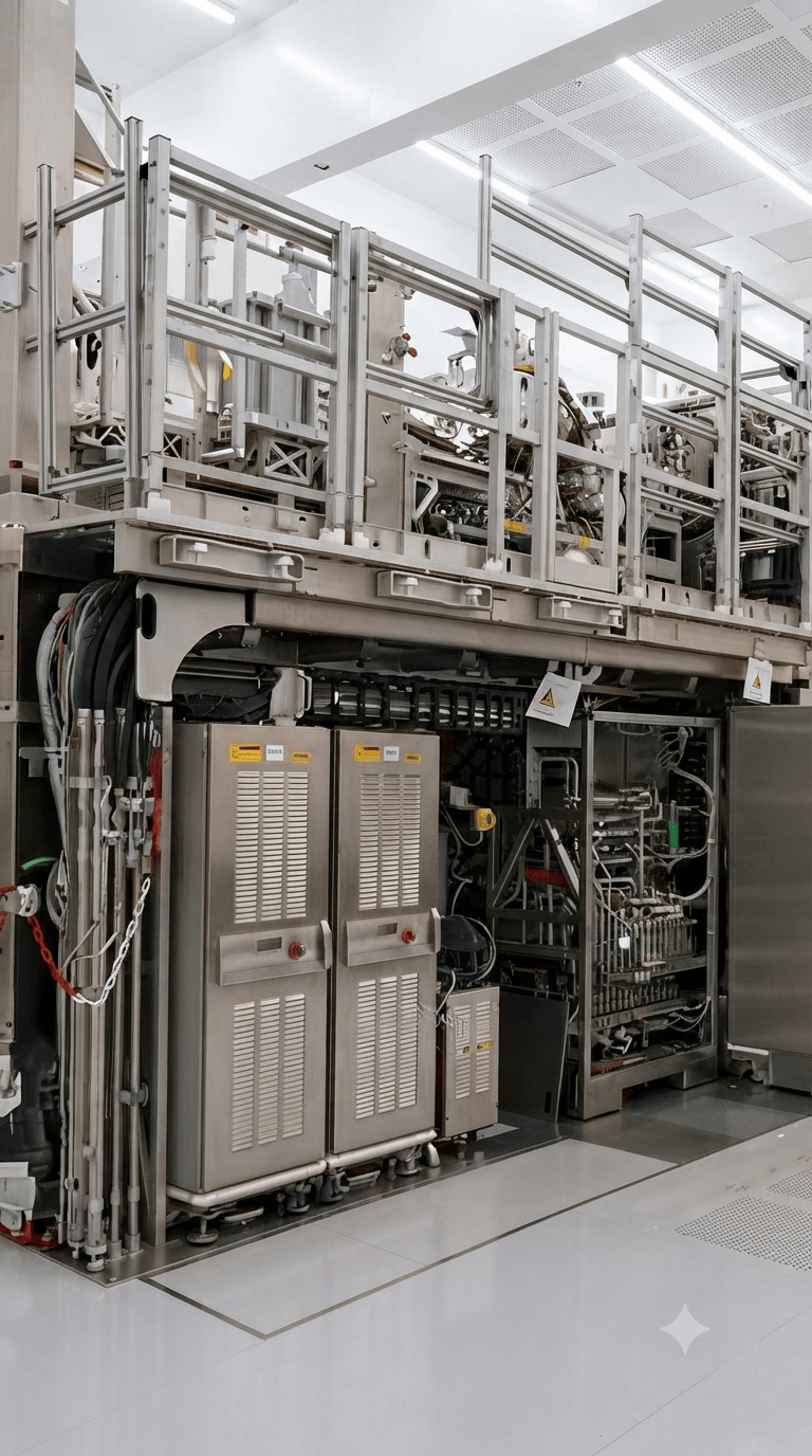
Since the project has not yet entered the construction phase, it will be necessary to monitor whether Samsung Electronics formally approves the investment, as well as the procurement arrangements for plant construction, cleanrooms, ultrapure water, specialty gases, power supply and distribution, exhaust treatment, and wafer manufacturing equipment. Only after the investment plan and construction timeline are officially confirmed will the new production capacity of 100,000 wafers per month enter the actual implementation stage.